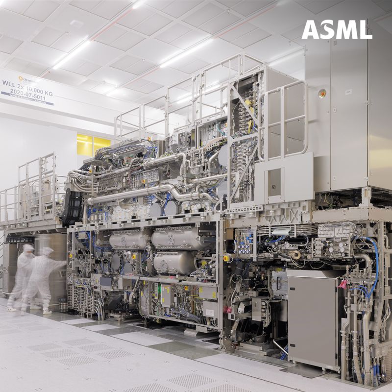
Samsung Electronics and ASML are expanding their semiconductor partnership around one of the most important technologies shaping the next generation of advanced chips: High-NA extreme ultraviolet lithography.
Samsung confirmed on September 8 that it will join an industry initiative developing next-generation 12-inch photomasks for High-NA EUV. The company also plans to introduce ASML’s High-NA EUV technology into high-volume DRAM manufacturing by 2028, which Samsung says would be a first for the industry.
What happened?
For decades, semiconductor manufacturers have relied on 6-inch photomasks. Photomasks contain the microscopic circuit patterns that lithography systems transfer onto silicon wafers during chip production.
High-NA EUV is the next step beyond the EUV systems already used to manufacture leading-edge processors and memory. Its higher numerical aperture allows finer features to be printed, helping chipmakers continue shrinking critical structures as conventional manufacturing becomes increasingly complex.
There is a trade-off, however. Current High-NA systems have a smaller exposure field, which can require large chip designs to be split and stitched together. The proposed move to larger 12-inch masks is designed to reduce those constraints while improving manufacturing productivity.
Why the Samsung-ASML partnership matters
Samsung says larger photomasks could improve fab productivity, lower manufacturing costs and remove stitching constraints, allowing chipmakers to make fuller use of High-NA EUV.
Reuters reports that ASML expects the larger-mask approach could improve the productivity of High-NA systems by about 40%. The broader industry is moving in the same direction: TSMC is also participating in the 12-inch mask effort, while SK Hynix is evaluating participation.
Samsung’s nearer-term target is particularly significant for memory. The company plans to bring High-NA EUV into high-volume DRAM production by 2028. High-NA’s improved resolution could simplify some manufacturing steps and help extend the roadmap for increasingly dense memory.
What does this mean for AI chips?
The announcement arrives as demand for advanced semiconductors continues to rise with the expansion of artificial intelligence infrastructure. AI accelerators, high-bandwidth memory and data-centre processors all depend on increasingly sophisticated semiconductor manufacturing.
High-NA EUV will not suddenly make tomorrow’s phones or laptops dramatically faster. Instead, it is part of the manufacturing foundation that could enable future generations of smaller, denser and more efficient chips.
That matters because improvements at the fabrication level can eventually flow into products consumers actually use: smartphones, PCs, graphics hardware, AI devices and cloud services.
When will High-NA EUV actually arrive?
The timelines are different for the lithography technology itself and the larger-mask initiative. Samsung is targeting High-NA EUV for high-volume DRAM manufacturing in 2028. Reuters reports that TSMC expects High-NA technology in advanced-node high-volume production from 2030.
The 12-inch photomask transition is a longer-term project. ASML plans to demonstrate a pilot line using the larger masks by 2031 and aims to have the technology ready for high-volume manufacturing by 2033.
The Tech Boom take
The important part of this announcement is not simply that Samsung is buying more advanced chipmaking equipment. Samsung and ASML are helping develop the manufacturing ecosystem needed to make High-NA EUV practical at scale.
With Samsung targeting DRAM production in 2028 and the industry working on larger photomasks for the following decade, the semiconductor race is increasingly being fought not only over chip designs, but over the tools and processes capable of manufacturing them economically.
Sources
- Samsung Global Newsroom — Samsung Electronics and ASML Expand Strategic Collaboration for Next-Generation Semiconductor Manufacturing, September 8, 2026.
- Reuters — ASML to work with major chipmakers to use latest tools for larger chips, September 8, 2026.